ZOTAC ZBOX PICO PI320 DISASSEMBLY
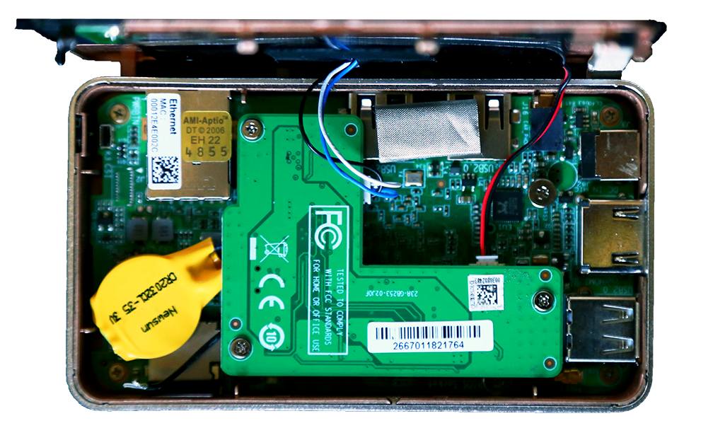
Considering all that can be found in the PI320, we were certain that this might be one of the most enjoyable system tear downs we have done to date. Both the top and bottom are a black moulded plastic and the top is held in place by clips that attach to the metal band that surrounds the unit. We DEFINITELY wouldn’t advise anyone following our lead because, as we did, you may find out the hard way that the WiFi panel is attached to that plastic and requires extreme care in removal. We ripped out the WiFi cable and a bit of soldering was in order on re-assembly.
At first glance, we could see a main PCB, accompanied by a ‘L’ shaped daughterboard, held in place by three screws. Taking a look at the bottom right, you can see the black WiFi wire that we ripped out.
Once we disconnected the remaining three wires, slightly tilting the unit allowed the PCB to fall out where we noticed a large metal heatsink connected to the bottom of the board. The removal of two screws allowed us to separate the heatsink from the PCB.
Looking at the bottom of the heatsink, we see three pieces of rubber that are used to conduct heat from the CPU, memory and capacitors. Also, on the bottom where a square is visible, we removed the thermal pad from the top of the Samsung eMMC chip.
Looking at the base of the PCB, we can identify four SKHynix DDR3L-1333 memory chips, each being 512GB in size with a product number of H5TC4G63AFR. The Intel Atom Z3735F ‘Bay Trail’ Quad Core CPU is just below that with the Ampak AP6383 chip to the right; this providing for 802.11N 2.4Ghz WiFi and BlueTooth 4.0. Just below the CPU and to the left is the Samsung 32GB eMMC 5.0 embedded flash controller.
This chip consists of 32GB high density MLC NAND, and a MMC controller in a 153-ball BGA package. Considering that this chip is smaller than that of a postage stamp, its ability is amazing. Anyone wishing to read up a bit on this chip can head over to the Samsung eMMC Overview page.
Examining the top of the PCB, there is a large square chip on the right side, this being an IDT multi-channel power management IC, specifically for the Intel Bay Trail Atom SoC. To the left of that, and left of the blue chip labeled ‘R47’ we see find the connector for the daughterboard. Also, the chip on the left and below the bar code is the Realtek ALC640 multi-channel stereo audio module.
Last but not least, we have the ‘L’ shaped daughterboard and it contains several Richtek RT9059 3A Ultra Low Dropout Voltage Regulators. Each is capable of supporting power as low as 0.8V.
 The SSD Review The Worlds Dedicated SSD Education and Review Resource |


Thats a pretty fast eMMC !
One would expect much lower speeds, considering the simplistic nature of the device.
One thing i do woder though. Since this is passivly cooled, how low is this throttling under load ?
So wait for this whit core m for 250 eu or 300 laptop whiti 5gen pentium.
Attach a little 5V battery pack to this baby and you have a very portable web server or private hotspot.
Great review! Just want to fix two typos:
1. It should read “2.4Ghz WiFi” instead of “1.4Ghz WiFi”.
2. It should read “Realtek ALC5640” instead of “Realtek ALCS640”.
Would I be able to change the memory chips, to allow for more ram? I’m asking because they are all soldered on.
‘They are all soldered on”