INTERNAL COMPONENTS
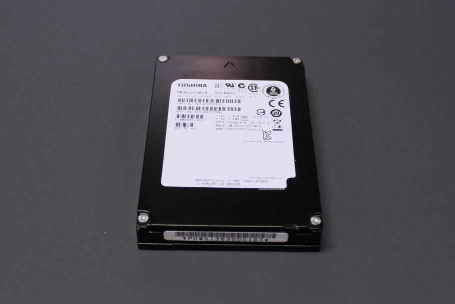
The MK4001GRZB is a stout little device, with quite a bit of heft to it. The metal casing that it is enclosed in is much heavier than any consumer SSD that we have ever evaluated, and there are also holes in the device that you will not see on any consumer devices on the market.
 These holes are aligned on the left bottom and designed to allow heat to escape as this SSD will generate a considerable amount of heat during operation, as all enterprise SSDs do. This heat must be wicked away from the device as effectively and quickly as possible to assure the longevity of the device. Toshiba has taken a very unique, and literally multilayer, approach to this issue.
 The key is in the different layers within the device. The SSD is built around an interior layer of very thick metal, which has thermal conducting pads attached. These pads are affixed to the NAND and capacitors that are placed next to it. There is a sandwich design, and a slot down the middle of the central housing that allows the connectors to mate together with the metal partition between them. All NAND flash memory dies, capacitors, cache chips, and the Marvell processor have these thermal conductive pads affixed to facilitate heat transfer.
The heat transfer also continues to the external casings, with thermal pads passing the heat through to the outside of the SSD for easy dissipation.
 On the rear of the two PCBs that are sandwiched together there are four capacitors that will provide enough charge to commit the writes to the NAND, should the device lose power. Also worthy of note is the long connector on the edge of the PCB, which mates with the connector below, through the slot in the middle metal layer of the SSD. This allows both PCBs to communicate with one another.
In the photo below, we can see 16 Toshiba TH58TAG8S2FBA8A modules of 32nm Toggle Mode NAND flash memory with a capacity of 32GB each. 400 GB is user addressable with the remainder committed to device over provisioning.
 On the other side of the PCBs the Marvell eight-channel 88SS9032-BLN2 SAS 6Gb/s controller can be seen above the two Micron D9LGK DDR3 cache memory chips that total 512MB. In the event of power loss the capacitors will enable this cache to be flushed to the device before total power loss.
 The SSD Review The Worlds Dedicated SSD Education and Review Resource |
Thanks for the detailed report. Can you compare/contrast this with the OWC enterprise drive, which is 1700 vs 6000 for the Toshiba. Is it worth 3 times the price? I do see the attention they paid to heat and don’t know if OWC has done the same homework, but the OWC drive does use an enterprise SandForce chip which should have the same features as the Marvell.
Awaiting arrival of the OWC SSD.
I guess the price difference is SLC vs eMLC, (correct me if I’m wrong) and their additional work on putting it together really well in terms of the heat dissipation. But in real terms I guess this comes down to longevity? It would be very interesting if you could do some applied but theoretical analysis of longevity comparisons. For example, if serving a database or web server with x writes and y reads per day how long would each last? I think the SLC is in the millions so that can be counted on for 5 yrs+ but the question is, with the features of the enterprise SF chip, what life can be expected there? The speed should be comparable, maybe with a slight bump for this drive in IOPS.