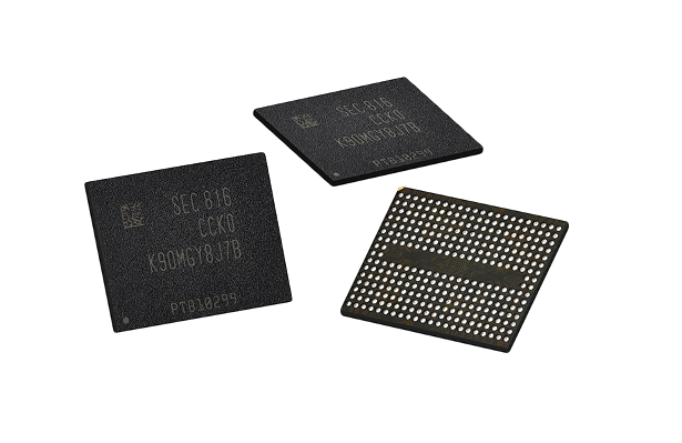
Samsung is announcing that they have begun mass-production of their fifth-generation V-NAND memory chips, supporting the fastest data transfer speeds currently available. This also represents the industry’s first use of the ‘Toggle DDR 4.0’ interface, enabling the transfer of data over the new 256Gb V-NAND at rates of up to 1.4Gbps. This represents a 40% increase over their prior 64-layer V-NAND.
 Samsung’s fifth-generation V-NAND stacks more than 90 layers of ‘3D charge trap flash’ (CTF) cells in a pyramid structure, and with microscopic channel holes drilled vertically throughout. These channel holes, at only a few hundred nanometers (nm) wide, provide more than 85 billion CTF cells that are each able to store three bits of data.
 Enhancements in Samsung’s V-NAND atomic layer depositing process have allowed for a more than 30% increase in manufacturing productivity. This cutting-edge process also allows for a 20% reduction in the height of each cell layer, minimizing crosstalk between cells and increasing the chips’ data processing capabilities.
 According to Kye Hyun Kyung, Samsung’s executive vice president of Flash Product and Technology, “Samsung’s fifth-generation V-NAND products and solutions will deliver the most advanced NAND in the rapidly growing premium memory market. In addition to the leading-edge advances we are announcing today, we are preparing to introduce 1-terabit (Tb) and QLC (quad-level cell) offerings to our V-NAND lineup that will continue to drive momentum for next-generation NAND memory solutions throughout the global market.”
 Samsung expects to quickly ramp up production of the fifth-generation V-NAND to embrace a wide range of market applications. Samsung continues to lead the adoption of high-density memory across key market segments that include enterprise servers, supercomputing and premium smartphones. Once again, the rest of the industry is left playing catch-up.
 The SSD Review The Worlds Dedicated SSD Education and Review Resource |