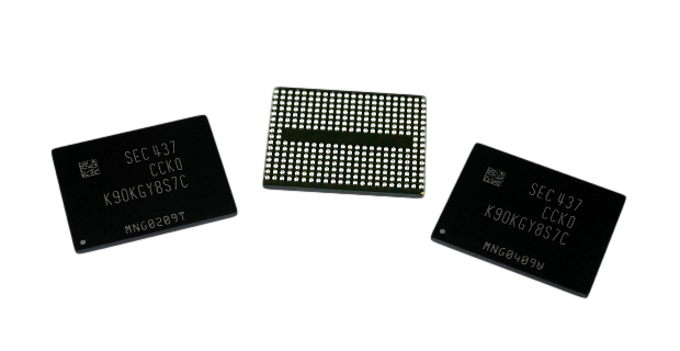
Samsung Electronics Co., Ltd., world-leading producer of advanced memory technology devices, is announcing that it has begun mass production of the industry’s first 3-bit multi-level cell (MLC) three-dimensional (3D) Vertical NAND (V-NAND) flash memory modules geared for use in solid state drive (SSDs). The 3-bit MLC V-NAND is Samsung’s newest second generation 3D V-NAND product, utilizing 32 vertically stacked cell layers per NAND chip. Each chip enables 128 gigabits (Gb) of memory storage.
According to Jaesoo Han, Senior Vice President of Memory Sales & Marketing at Samsung, “With the addition of a whole new line of high density SSDs that is both performance- and value-driven, we believe the 3-bit V-NAND will accelerate the transition of data storage devices from hard disk drives to SSDs. The wider variety of SSDs will increase our product competitiveness as we further expand our rapidly growing SSD business.”
Samsung’s latest V-NAND chip structure has each cell electrically connected to a non-conductive layer, using charge trap flash (CTF) technology. Each cell array layer is stacked vertically on top of one another, forming chips with multi-billions of cells.
 Image source: spansion.com / Flash Memory Summit 8-13-13
Samsung first introduced its 3D V-NAND (24 layers) in August of 2013, followed by its second generation 3D V-NAND (32 layers) cell array structure in May of this year. With this launch of 32-layer 3-bit V-NAND, Samsung extends its lead in the 3D memory arena, and continues to speed the evolution of V-NAND technology and production.
With the use of 32 layers of 3-bit-per-cell arrays stacked vertically, Samsung has raised the efficiency of its memory production. Compared to Samsung’s own 10nm-class 3-bit-per-cell planer (2D) NAND flash modules, the new 3-bit V-NAND has more than doubled wafer productivity.
Market adoption of V-NAND memory should expand considerably with Samsung’s industry-first 3-bit 3D V-NAND flash. This will lead to production of SSDs that are not only suitable for general PC use, but should also efficiently address the high-endurance storage requirements of today’s servers.
 The SSD Review The Worlds Dedicated SSD Education and Review Resource |

That’s a three bit technology.
I’m confused… That’s only 16 gigabytes per chip. Does this article have the specs wrong? 16GB is nothing exciting, even if they meant 16GB per layer… With 32 layers, that’s still only 512GB.
Yeah 512 GiB per. package. A normal SSD contains 4, 8 or 16 packages. So that is an SSD with 2 TiB, 4 TiB or 8 TiB of storage depending on how many packages are used.
A 2tb in a nice laptop with ddr4 a quad core skylake 45w 128mb L4 GT4e gpu. I’ll be set, and at light bulb wattages, much excite. Now if only the rest of the industrial world could match in efficency..
Dalmus: no the article does not have the spec wrong and yes it is exciting. 4, 8 or 16 gigabyte per chip is “commen”. A package normally contains more than one chip. Samsung have previously packaged 16 chips (64 gigabits) in one package for a total of 128 gigabytes per package. That is a lot of storage in a small space.
https://www.samsung.com/global/business/semiconductor/support/package-info/package-datasheet/flash