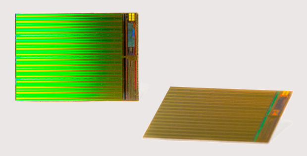
Micron Technology, Inc., and Intel Corporation are announcing availability of their new 3D NAND technology, currently the world’s highest-density flash memory. This enables development of computing devices with significantly increased storage capacity, including for laptops, datacenters, and virtually every mobile device, such as tablets and smartphones.
This latest 3D NAND technology was a collaborative development between Intel and Micron, and it stacks storage cells vertically with extreme precision to create a storage device that is claimed to have three times more storage capacity than competing technologies. Larger storage capacity occupying less space brings remarkable cost savings, high performance and low power usage to meet the needs of both enterprise datacenters and a broad range of consumer mobile computing devices.
2D (planar) NAND flash memory production has nearly reached its downward-scaling limitations. The new 3D NAND technology will allow flash storage solutions to continue to grow in capacity, while shrinking in size. This should accelerate widespread adoption of flash storage, and allow Moore’s Law to continue on its current trajectory in the form of continued cost savings and performance gains.
According to Brian Shirley, Micron’s vice president of Memory Technology and Solutions, “ Micron and Intel’s collaboration has created an industry-leading solid-state storage technology that offers high density, performance and efficiency and is unmatched by any flash today. This 3D NAND technology has the potential to create fundamental market shifts. The depth of the impact that flash has had to date – from smartphones to flash-optimized supercomputing – is really just scratching the surface of what’s possible.”
According to Brian Shirley, Micron’s vice president of Memory Technology and Solutions, “ Micron and Intel’s collaboration has created an industry-leading solid-state storage technology that offers high density, performance and efficiency and is unmatched by any flash today. This 3D NAND technology has the potential to create fundamental market shifts. The depth of the impact that flash has had to date – from smartphones to flash-optimized supercomputing – is really just scratching the surface of what’s possible.”
Intel and Micron’s choice of memory cell is the floating-gate design, which is the universal design used in conventional planar (2D) flash memory. Years of high-volume production has refined the floating-gate cell, and using it for the 3D NAND enables greater performance, higher quality and higher reliability.
This 3D NAND technology is created by stacking 32 layers of flash cells vertically, which achieves 256Gb of multilevel cell (MLC) memory or 384Gb of triple-level cell (TLC) memory within a standard die package. With these capacities, we could easily see gumstick-sized SSDs packing more than 3.5TB of flash storage, and more than 10TB of flash storage in a single 2.5” form factor SSD. With vertical stacking providing the larger capacity, individual cells can be larger, resulting in increased performance, as well as increased endurance. This could result in even TLC flash being a good fit for datacenter usage.
A 256Gb MLC version is currently sampling with key partners, and the 384Gb version is anticipated to begin sampling later this spring. Initial runs have already started on the fab production line, and both the 256Gb and the 384Gb will be in full production by Q4 of 2015. Both Micron and Intel are also developing their own SSD solutions based on this latest 3D NAND technology, with products from both expected to be available within a year. You can view Micron’s press release announcing the new 3D NAND technology in its entirety here.
 The SSD Review The Worlds Dedicated SSD Education and Review Resource |

