So our friends at MyCE sent us an e-mail early this morning, detailing their exclusive discovery of Intel’s latest SSD roadmap, a roadmap that provides plenty of clues as to where Intel is going in the SSD realm. First and foremost, congrats to JW and the MyCE crew for grabbing this one away from Chinese VR-Zone, the undisputed the ‘leaked roadmap leader’. Having examined several pages of this purported Intel document closely, I will be the first to say that it raises just as many questions as it provides answers and I’de like to walk you through each, a page at a time, with some personal thought on the document. Before we go further though, a BIG THANKS to the MyCE Team for allowing our publishing of all shots and head on over there to get their perspective on things.
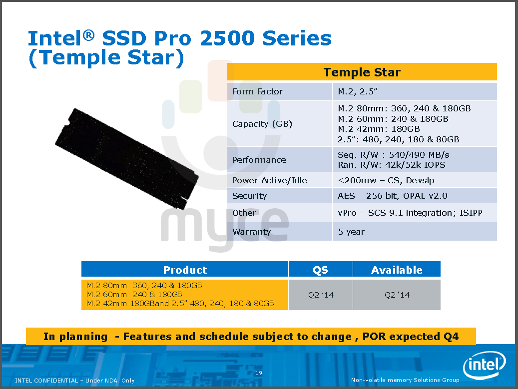
Looking at this first slide, I was a bit shaken. The picture of the M.2 SSD that is blacked out on the left, displays an PCIe X4 M.2 SSD (notice the single M Key), yet there is no mention of those blazing LSI SandForce speeds on the right. As well, the low IOPS spec is definitely not characteristic of new LSI SandForce performance and we know that Intel and LSI are as close as can be right now. There are definitely hints of LSI SandForce features, to include Devslp, AES 256-Bit encryption and Opal 2.0 compliance, but there is almost enough left out of this to make us wonder now isn’t there?
This slide lays out Intel’s new enterprise offerings, much the same as it did last round, with a choice of Intel’s best HET MLC NAND flash memory or the typical MLC that we are all used to. The product name DC P3700 definitely caught my eye though because of its similarity to the LSI SandForce SF3700 flash controller capable of 1.8GB/s. Seeing Q2 2014 as a release date was a bit encouraging, although we believe that there will be some great displays by Intel, and all other LSI SandForce partners, at CES in January.
Now we are getting somewhere. Mark my words that Native-PCIe performance is going to take its toll on SATA in the next few years and the race starts here. Displaying 2.8GB/s read and 1.7GB/s write specifications would lead us to believe that this PCIe SSD is based on two SF3700 Flash controllers and that Intel has followed their traditional ‘hard-core’ test results in listing speeds. We have to admit though that even 450,000 IOPS for two controllers seems a bit out of place, especially when the write performance is half that.
The DC P3500 has much the same specs, however, you might note that low 4K write IOPS have dropped down to a mere 40,000. That PCIe card is definitely a thing of beauty though.
At the end of the day, we seem to be brought back to the Temple Star which will reach the hands of the consumer as a 2.5″ or M.2 SSD. Perhaps the most disappointing thing here is the fact that there is no evidence of it, or a similar version, coming out in those now familiar speeds of 1800MB/s read and write.
A definite positive is that access and pricing will most likely provide the consumer the opportunity to purchase the DC P3500 PCIe card, just as we saw with the DC S3500. Add to that the fact that, if it was actually running on 2 x SF3700 flash controllers as we believe, initial benchmarks for both read and write just might be somewhere around the 3GB/s mark with 450K IOPS.
 The SSD Review The Worlds Dedicated SSD Education and Review Resource |


Personally, I hope it starts raining SF-3700s. Some speculation says it’ll be 2H until it hits mass availability. Hoping LSI is working on a raid controller built just for a pair of SF3700s on a pcie card.